The ability to read in, export and synchronize FPGA designers HDL and constraint files ensures full consistency during the iterative FPGA PCB I/O concurrent design process. Incidentally, it also allows creating high pin count FPGA PCB parts ready for instantiation in minutes.

How Integrated FPGA-PCB I/O Co-Design Accelerates PCB Design and Reduces Costs
Integrated FPGA-PCB I/O Co-Design
- Reduce the total product design cycle time by changing a serial process into a concurrent process.
- Decrease PCB manufacturing costs by eliminating PCB signal layers.
- Eliminate PCB re-spins due to out-of-date FPGA symbols on the PCB.
- Remove the costs associated with creating and maintaining the FPGA symbol(s) for the PCB schematic.
- Utilize high-speed performance optimization.
Integrated FPGA PCB IO Co Design
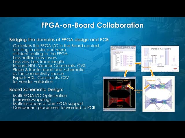
FPGA I/O optimization provides an extensive set of easy to use functionality created to fully support schematic and PCB engineers with their FPGA-on-board integration. Furthermore, concurrent design processes provide greater accuracy and speed. Correct-by-construction FPGA I/O assignment allows for pin swapping and layout-based I/O optimization within the PCB process to significantly reduce the time-to-market of PCB systems and manufacturing costs, both absolutely key in today’s fast paced and ever-changing design environment.
PADS Pro FPGA-PCB Co-Design Option
Interested in getting more details on this FPGA-PCB Co-Design Option, let us know by filling in this form.
We can provide you with pricing details as well a detailed datasheet.