Many of today’s product designs include multiple RF modules, with high-speed digital and analog circuitry in tight proximity on the same board. For complex system-level designs, as much as 75% of the total cycle time can be spent on RF circuits, making it imperative to find ways to drive efficiency through this process.

PADS Professional
RF-Design
- Ground stitching vias to shield RF circuits
- Restrictive clearance rules specific to RF
- Automated RF circuit arrangement and grouping
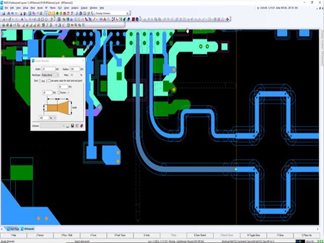
- Meanders
- Via-stitching for easy creation of co-planar wave guides
- Flood regions with vias according to your rules
- The import of complex RF shapes
- Chamfered corners
RF and PCB Parallel Design
Today’s PCB designs often include multiple RF modules, with high-speed digital and analog circuitry in tight proximity. Up to 75% of total cycle time can be spent on RF circuits. The PADS Professional combination of engine and modeling technologies enables you to implement a fast, efficient, unified design flow.
Accelerating RF PCB Design in a 5G World - Whitepaper
Billions of IoT devices coming online in the coming tears will require RF design capabilities that support ultra-fast 5G speeds.
Interested in getting a whitepaper, let us know by filling in this form.